Project 8
555 Blinker PCB
By Patrick R Cabanban
Overview
You have explored circuit design and prototyping through breadboards and perfboards. This time, you will explore the manufacturing of more sophisticated circuit prototypes and finished products: You will create a printed circuit board (PCB) of the all-too-familiar 555 Blinker circuit with the software KiCad.
Concepts
Printed Circuit Boards (PCB)
When electronics are more complex or are ready for production, we typically use printed circuit boards or PCBs. Nearly every device, from a digital alarm clock to laptop computer, uses a PCB. It is a board designed with CAD software that connects individual components.
The benefits of PCBs over prototyping boards are numerous: They're more compact, more reliable, and enable complex circuit design. Above all, they are easy to mass produce.
To learn more about PCBs and how they are constructed, view the lecture material here.

PCB Design Overview
When it is time to design your PCB, there are two major components of the operation: (1) Schematic capture - converting your prototyped design and circuit drawings into a digital schematic. (2) PCB Layout Design - placing components and routing conductive tracks in a virtual layout of your PCB. You can learn exactly how this process works in the KiCad EDA software by viewing our PCB Design with KiCad workshop material here.
Installing KiCAD 7.0
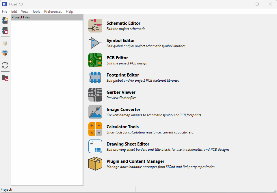
To complete this project, you will download the PCB design software KiCad (version 7.0.11).
| Windows | Download |
| Mac | Download |
- Download the installer from the link appropriate to your OS.
-
Launch the installer. Click Next.
-
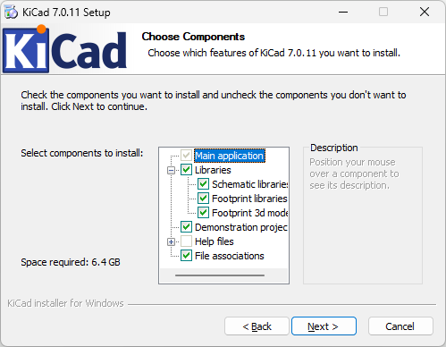
When the Choose Components dialog appears, make sure all but the “Help files”
components are selected. Then, click Next.
-
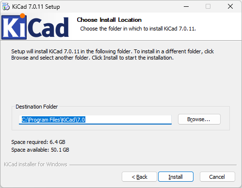
Select the Install Location. The default setting is usually acceptable. Then,
click Install.
- The installation is complete! The fun starts now.
Requirements
For readers who are enrolled in the course: In order to receive full marks on your project submission, make sure it meets the following minimum requirements.
-
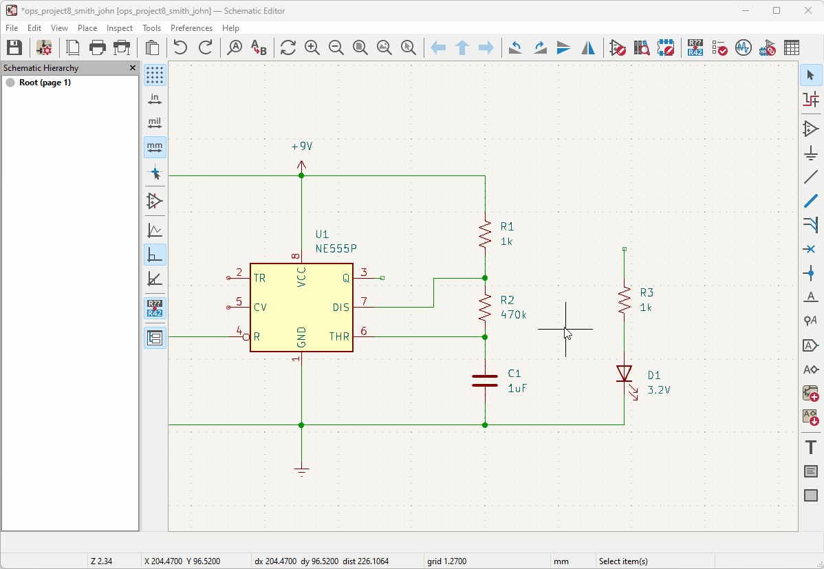
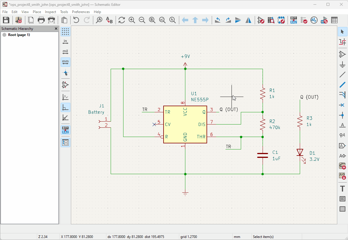
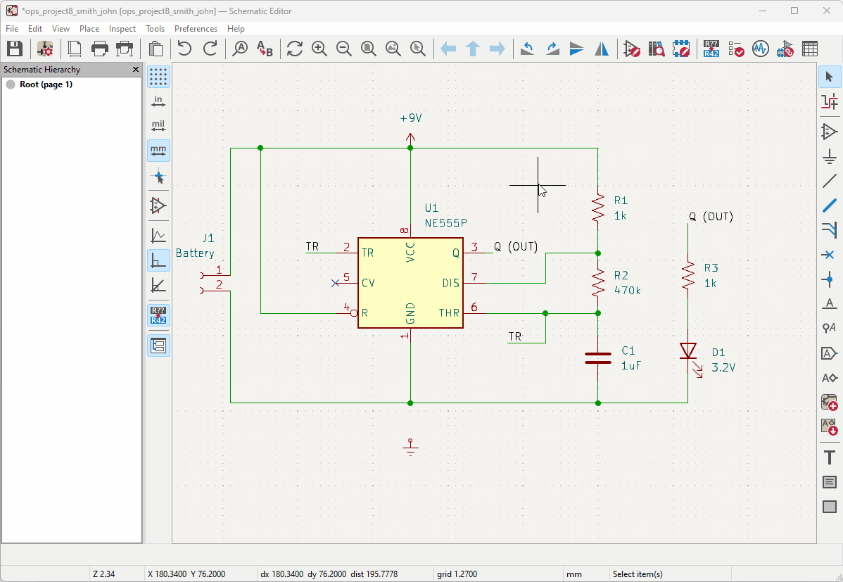
You must create a full schematic that replicates the provided 555 Blinker Circuit diagram
- The schematic must pass the Electronic Rules Check (ERC) for all but the error: “Input Power pin not driven by any Output Power pins.”
-
You must design a PCB from the 555 Blinker Circuit schematic you create
- The PCB layout must pass the Design Rules Check (DRC)
- The symbols and footprints used in the schematic and PCB must match those listed in the Parts section of the project specification
Parts
This is not a physical parts list. The following parts will be used in the PCB EDA application.
| Part | Symbol | Footprint Library | Footprint | |
|---|---|---|---|---|
| x2 | Header, 2.54mm, Female, 1x2 | Conn_01x02_Socket | Connector_PinHeader_2.54mm | PinHeader_1x02_P2.54mm_Vertical |
| x1 | NE555P IC | NE555P | Package_DIP | DIP-8_W7.62mm |
| x1 | Resistor, 1kΩ | R_US | Resistor_THT | R_Axial_DIN0207_L6.3mm_D2.5mm_P7.62mm_Horizontal |
| x1 | Resistor, 470kΩ | R_US | Resistor_THT | R_Axial_DIN0207_L6.3mm_D2.5mm_P7.62mm_Horizontal |
| x1 | LED, 3.2V | LED | LED_THT | LED_D3.00mm |
| x1 | Capacitor, 1µF | C | Capacitor_THT | CP_Radial_D4.0mm_P2.00mm |
Schematics

Instructions
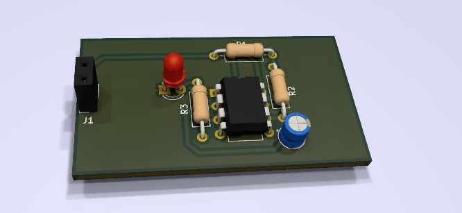
Each checkpoint guides you through the process of designing the 555 Blinker circuit, which should look something like this upon completion:
Make sure to save your progress frequently. Nothing is more infuriating than trying to recover lost data and lost time.
You should also do yourself the favor of using a mouse. Suffice to say, KiCad is unkind to touchpad users (and if you are using a pointing stick, something is wrong with you.)
And with that, let's get started!
Checkpoint 1
-
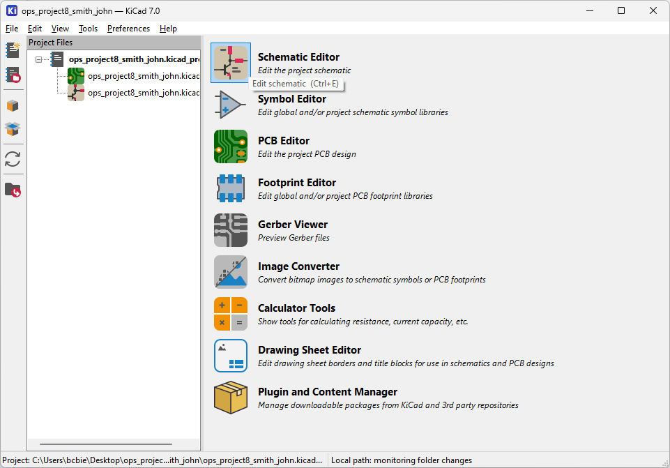
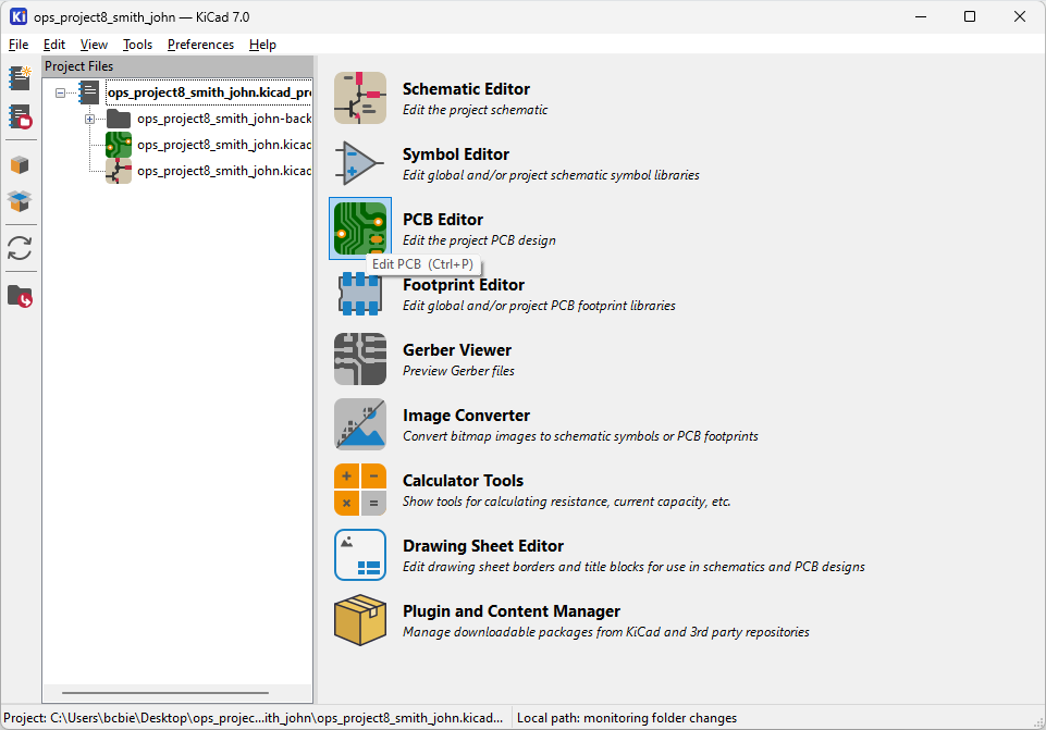
Open KiCad 7.0 to launch the Project Manager and create a new
project. Name the
project file using the following format:
“ops_project8_lastname_firstname.kicad_pro”
-
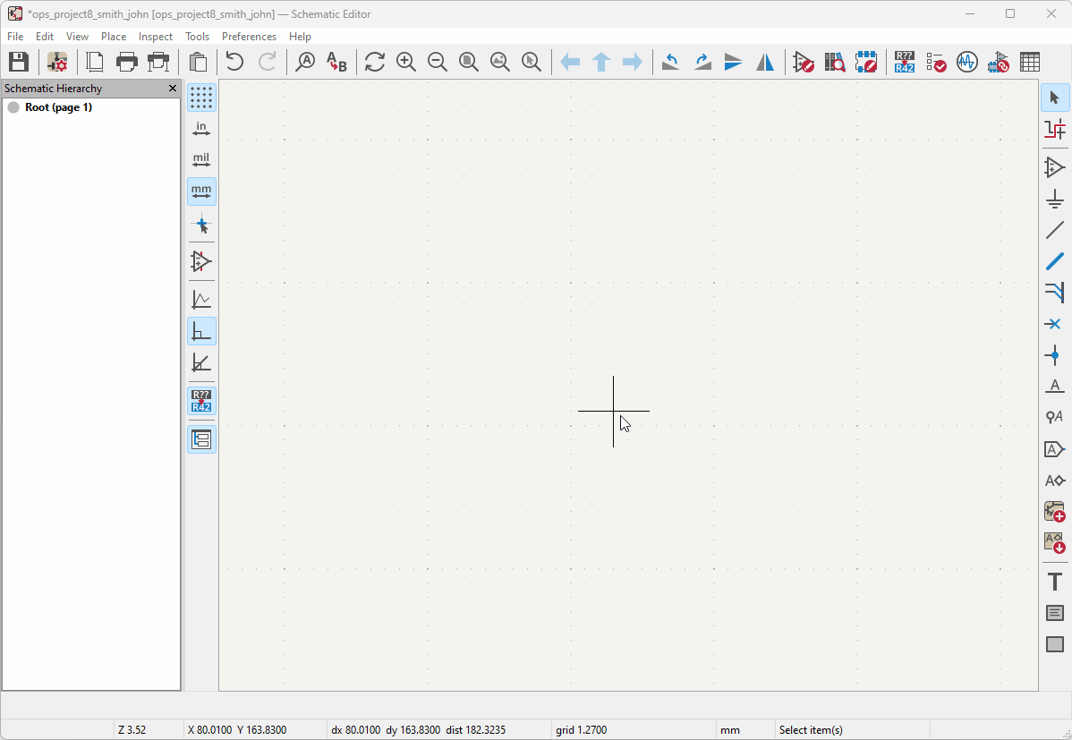
Now that you have created a project, open the Schematic Editor (or press
Ctrl+E, Mac: ⌘+E) to launch the schematic
capture application.
-
Click on Add Power Symbol
 (or
press P) to add the
+9V (VCC) and Earth schematic symbols.
(or
press P) to add the
+9V (VCC) and Earth schematic symbols.
 Need to zoom in or out? Use the mouse scroll wheel or select one of the following options from the menu bar at the top of the application:
-
Click on Add Symbol
 (or press A) and add each of the schematic
symbols listed in the Parts section of the
project
specification.
(or press A) and add each of the schematic
symbols listed in the Parts section of the
project
specification.
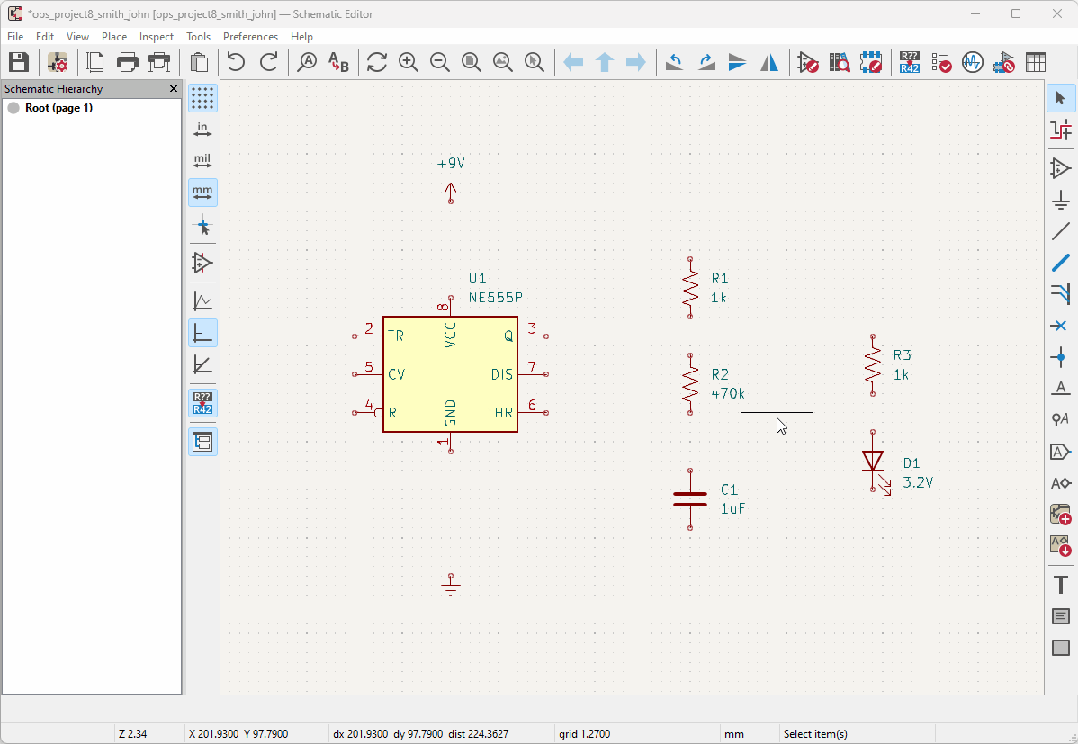
 Moving Symbols: You can move symbols by selecting them, then holding down the left mouse button, and moving the cursor. You can also select the symbol, press M, then move the cursor.
 -
For each valued component (resistors, capacitor, LED), right click on the component, and select
Properties (or press E).
Edit the Value field in the Symbol Properties dialog to be the corresponding component value in Ohms, Farads, etc.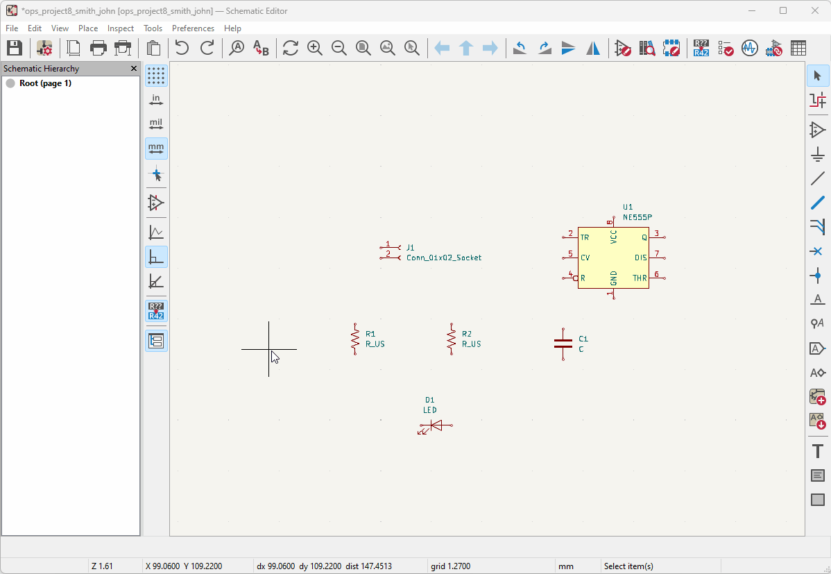 The value scheme is as follows:
{base value} {scale} {unit}
scale (power of 10): p: 10-12, n: 10-9, u: 10-6, m: 10-3, k: 103, M: 106, G: 109
unit: Capacitors: F, Inductors: H, Resistors: None
Ex. A capacitance of 1*10-6F would be denoted as 1uF.
In this example, {base value = 1} {scale = u} {unit = F} -
Open the Footprint Assignment
 tool. For each component symbol, assign a
footprint. The symbols' footprints (and their
footprint libraries) are defined in the Parts section of the project specification.
tool. For each component symbol, assign a
footprint. The symbols' footprints (and their
footprint libraries) are defined in the Parts section of the project specification.
After assigning each component, select Apply, Save Schematic & Continue to save your progress.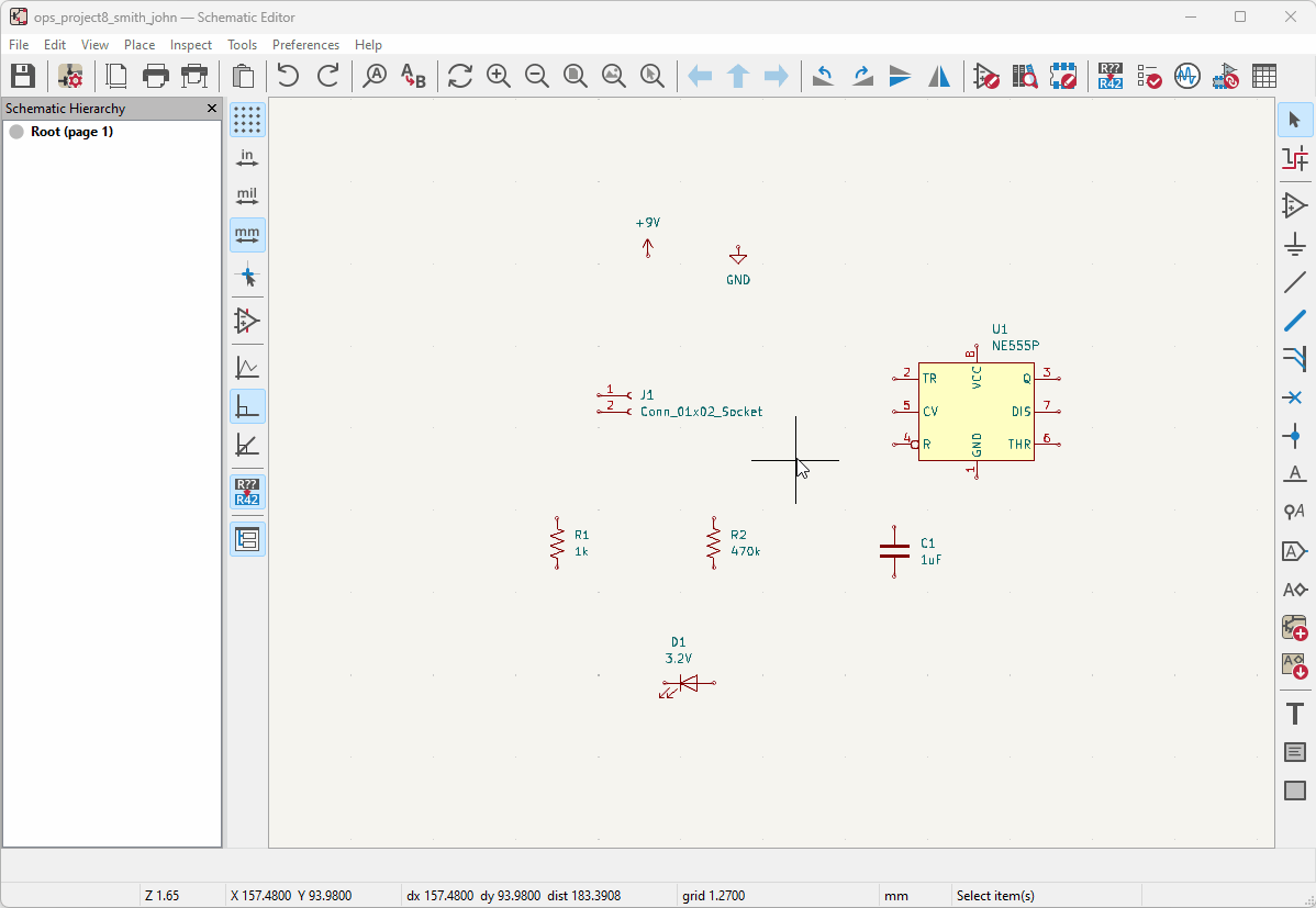 After footprints are assigned to symbols, you can copy (Ctrl+C, Mac: ⌘+E) and paste (Ctrl+V, Mac: ⌘+V) symbols and their footprint assignments will be copied over as well
 -
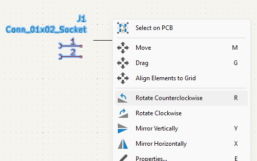
Move symbols and rotate them in preparation to connect them with wires. If a symbol is in the
wrong orientation right
click on the component and select Rotate Counterclockwise (or press
R) to rotate it 90 degrees
counterclockwise.
-
Complete the circuit defined by the provided schematic. Select the Wire
 button
(or press W) to create connections
between components and other wires. Connections between two wires are indicated by a dot.
button
(or press W) to create connections
between components and other wires. Connections between two wires are indicated by a dot.
-
Add net labels
 to
avoid crossing wires. Net labels are basically invisible
connections; they help clean up the
schematic.
to
avoid crossing wires. Net labels are basically invisible
connections; they help clean up the
schematic.
-
Add no-connection flags
 to indicate which pins/leads are to be left
unconnected. This is important for when we run
verification tools later.
Run the Annotate Schematic tool
to indicate which pins/leads are to be left
unconnected. This is important for when we run
verification tools later.
Run the Annotate Schematic tool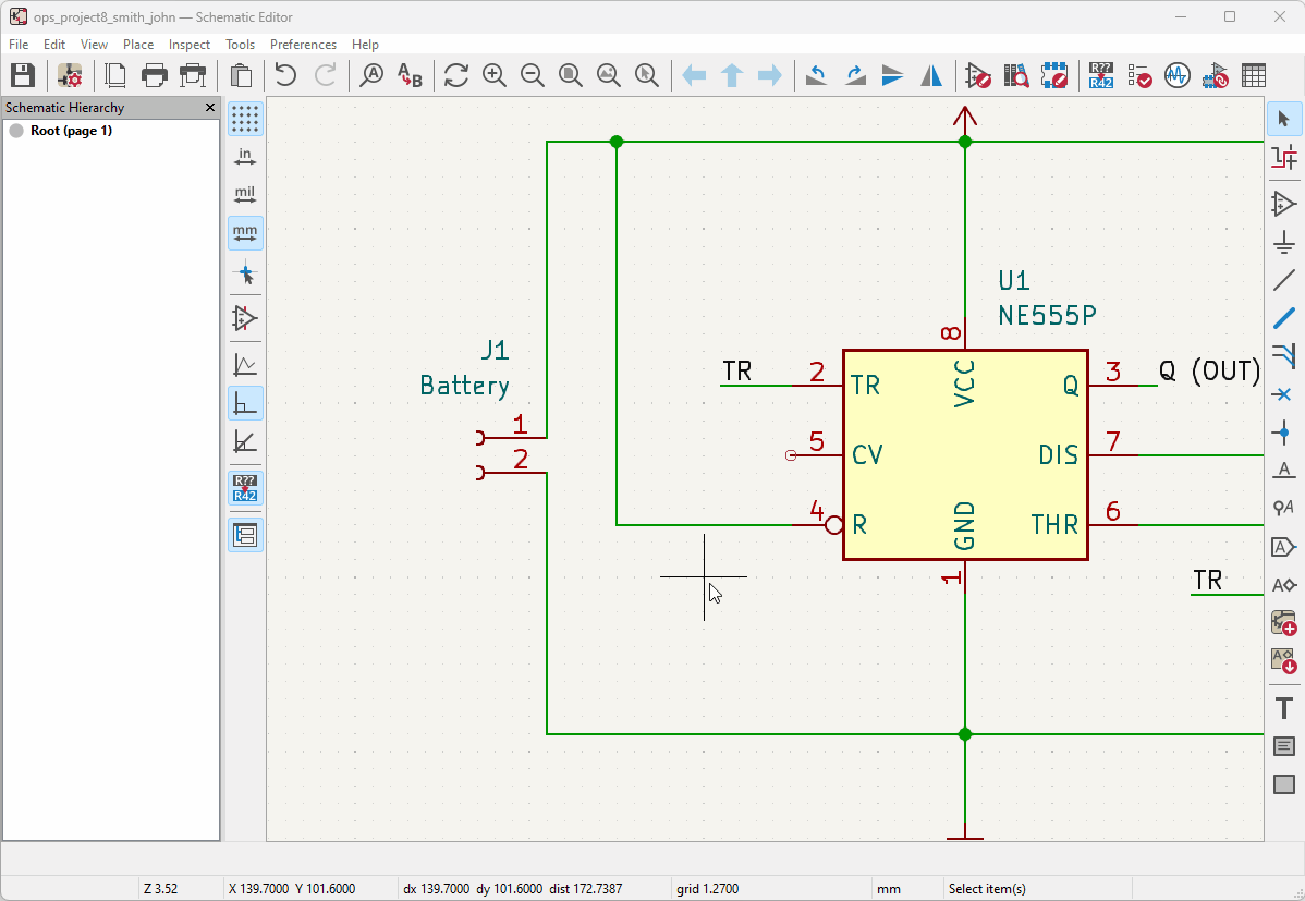
Checkpoint 2
-
Open the Annotate Schematic
 tool and select Annotate to name
the remaining symbols which have been marked erroneously
with “?”.
tool and select Annotate to name
the remaining symbols which have been marked erroneously
with “?”.
-
You will now verify the schematic. Open the Electrical Rules Check (ERC)
tool
 and select Run ERC
 There should be no violations except for Error: Input Power pin not driven by any Output Power pins.
Checkpoint 3
-
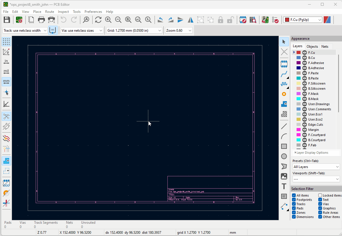
Return to the Project Manager window and open the PCB Editor
(or press Ctrl+P, Mac: ⌘+P).
-
Though this step is not required for your project, you can configure the stackup and add
manufacturer design constraints
by selecting File → Board settings
-
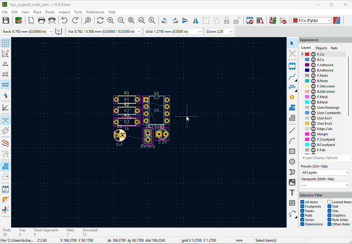
To generate the components specified by your schematic, open the Update PCB
 tool (or press F8) and select Update PCB
The component footprints will then be generated and follow your cursor until you left click to confirm their initial placement.
-
Now, you need to set the track and via sizes. Disable the Use Existing Track
Width..
 option by
selecting the button until it is no longer highlighted. Then, open the Track use
netclass width
dropdown and select Edit Pre-defined Sizes
option by
selecting the button until it is no longer highlighted. Then, open the Track use
netclass width
dropdown and select Edit Pre-defined Sizes
Add the following pre-defined sizes:
Traces with 40 mil width must be used for power and ground lines.Tracks (Width) Vias (Diameter/Hole) 40 mil 30mil/20mil 30 mil
Traces with 30 mil width must be used for signal lines
Vist the Track use netclass width and Via use netclass sizes dropdowns and select one of the newly populated options. (Change between the options as necessary when you route the traces.)
-
Create the board outline. Select the Edge.Cuts layer then use one of the shapes
tools to create the outline. Remember to
return to the F.Cu (Front Copper) layer when done. A board shape of ~60x35mm is reasonable for this project.
-
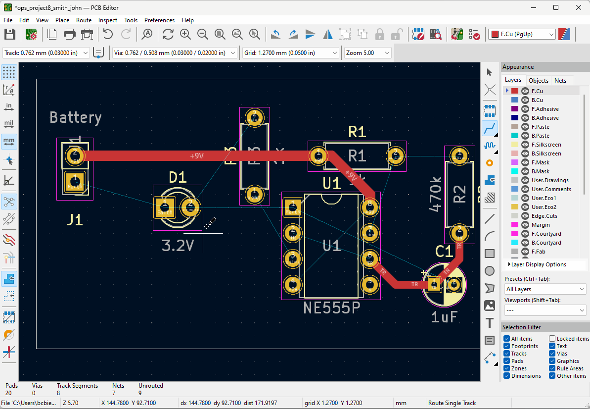
Space out your components a reasonable distance and create the traces. Select Route Tracks
 (or press X) and begin
drawing traces between pads which are connected by the
ratsnets.
(or press X) and begin
drawing traces between pads which are connected by the
ratsnets.
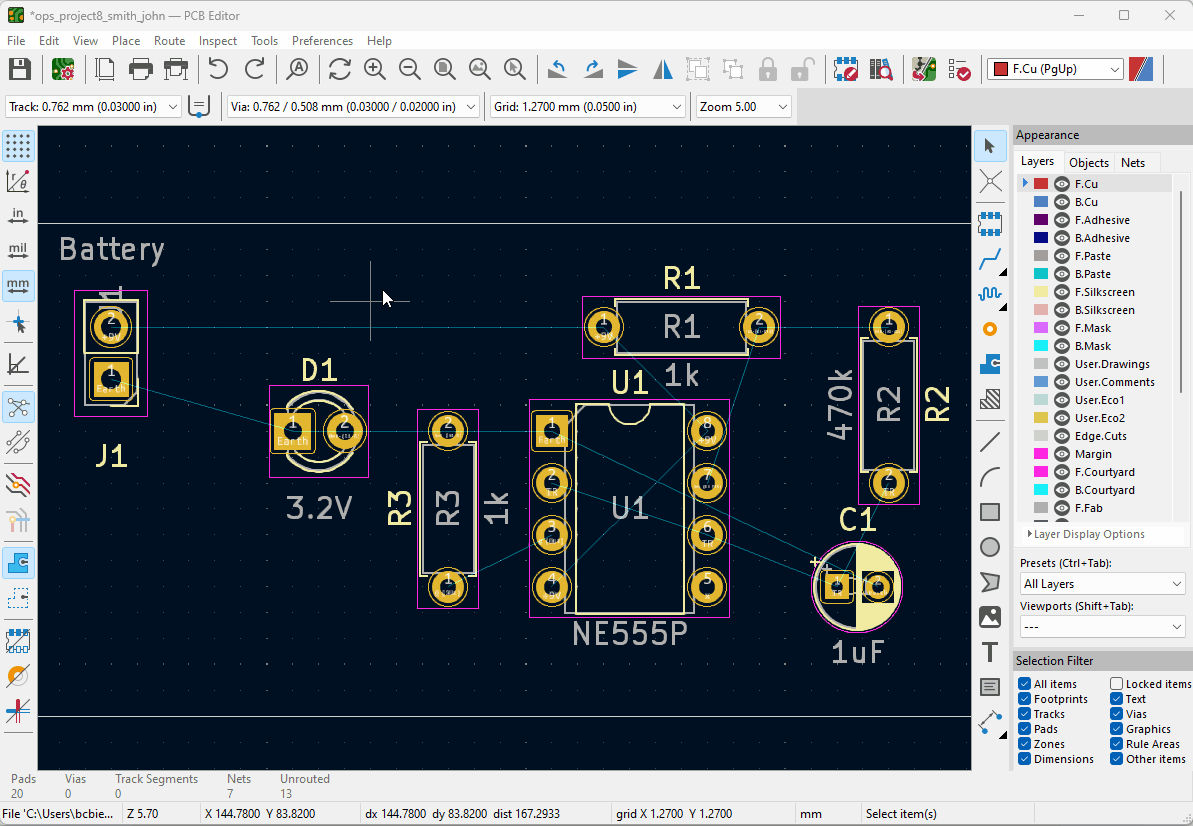 Remember to change the trace width according its use case. Power/Ground lines should be larger width than signal lines.Leave the ground pads unconnected.Pro tip: Avoid routing traces with 90 degree angles, and use 135 degree tracks instead.
Ex. The connection between NE555P Pin 6 to C1 Pin 1 maintains a 135 degree track. -
In the event two traces on the same layer must cross paths, you may instead create one of the
traces on the B.Cu (Back
Copper) layer.
Use the Add Via tool (or press
Ctrl+Shift+V, Mac:
⌘+Shift+V) to place vias which may connect traces of different layers.
(or press
Ctrl+Shift+V, Mac:
⌘+Shift+V) to place vias which may connect traces of different layers.
-
With all but the ground pads connected, you will create the ground fill. Select Add Fill
Zone
(or press Ctrl+Shift+Z
Mac: ⌘+Shift+Z). A dialog will appear:
Select both the F.Cu and B.Cu layers as well as the Earth net. Then, select Ok.
Now, left click to draw the closed area in which the fill will be created.
When the fill zone is created, press B to fill.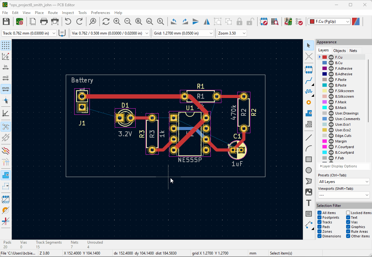
-
If you wish to add text to the PCB, select the F.Silkscreen layer. Then, use
the Add Text Item
tool
 (or press
Ctrl+Shift+T, Mac: ⌘+Shift+T) to generate and place textboxes
on the silkscreen.
(or press
Ctrl+Shift+T, Mac: ⌘+Shift+T) to generate and place textboxes
on the silkscreen.
Alternatively, you may write text to the back of the PCB by selecting the B.Silkscreen layer instead.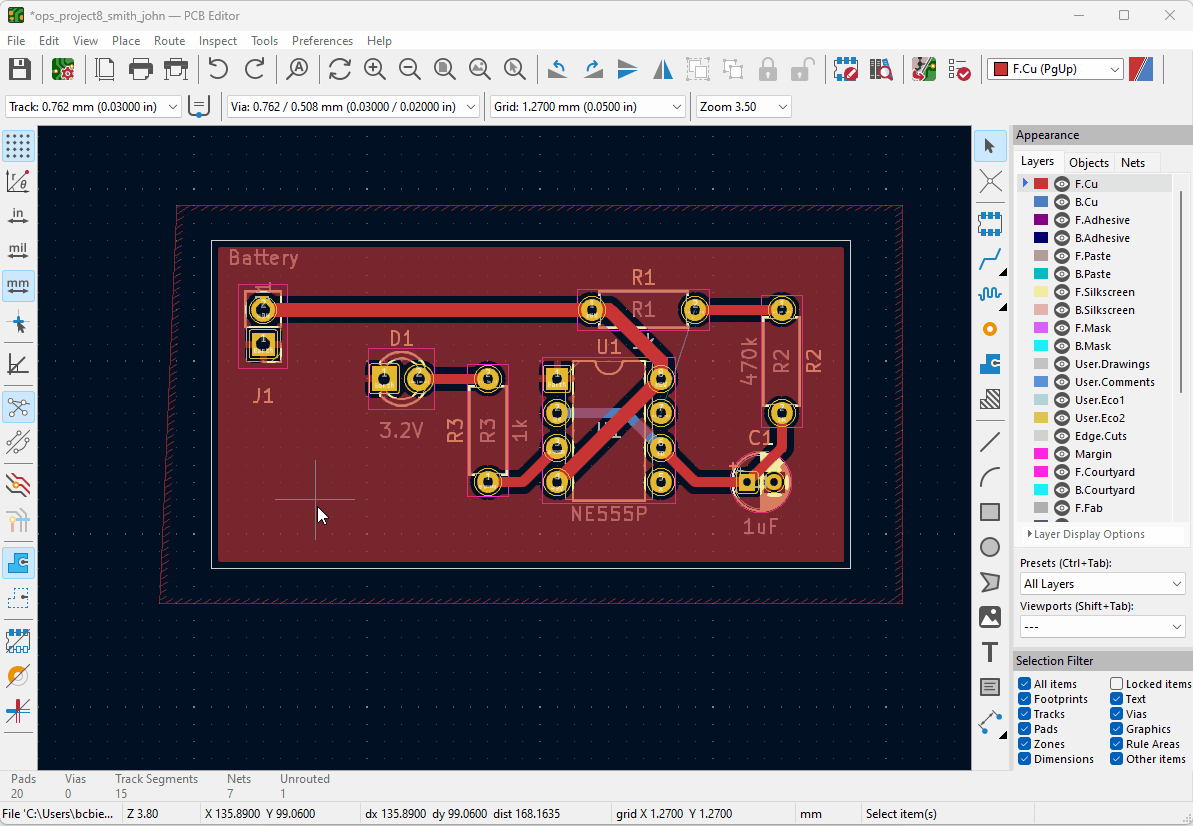
Checkpoint 4
-
Now to verify the PCB layout. Open the Design Rules Checker (DRC) tool and
select Run DRC. There should be no
violations.

Checkpoint 5
-
As a final checkpoint, you will generate the manufacturing files for your project. Select the
Plot tool. Then, choose an
Output directory. It should be a new folder called “gbr” in
your project folder.
Now, select Plot tool.
Then, select Generate Drill Files… to open a new dialog where you will select
Generate Drill Files
again.
tool.
Then, select Generate Drill Files… to open a new dialog where you will select
Generate Drill Files
again.
Close all the dialogs. You are done!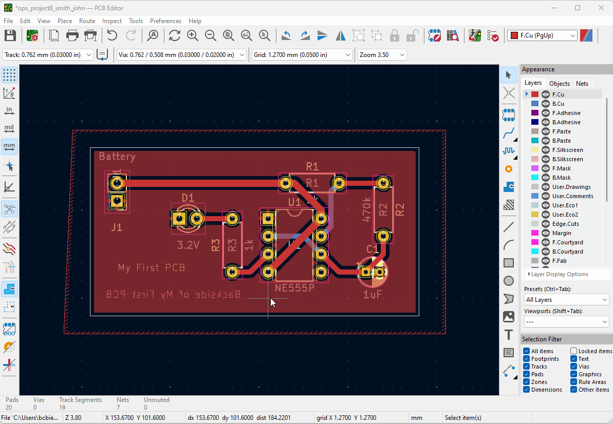
Deliverables (Enrolled Students Only)
Students enrolled in the course must submit the following deliverables to the corresponding Canvas course assignment.
Compress the KiCad project folder as a .zip. It must contain the following:
- KiCad Project File (.kicad_pro)
- KiCad PCB File (.kicad_pcb)
- KiCad Schematic File (.kicad_sch)
- Folder containing the manufacturing and drill files
Rename the zip file using the format “ops_project8_lastname_firstname.zip” Then, submit the zip file to the Project 8 Canvas assignment.